Engineers at the University of Wisconsin-Madison have devised a method to grow graphene nanoribbons directly on top of silicon wafers for more powerful and energy-efficient computers.
Smaller, better semiconductors have consistently allowed computers to become faster and more energy-efficient than ever before. The 18-month cycle of exponential increases in computing power that has held since the mid-1960s called Moore’s Law has leveled off. That’s because there are fundamental limits to integrated circuits made strictly from silicon — the material that forms the backbone of our modern computer infrastructure.
However, engineers at the University of Wisconsin-Madison are turning to new materials to lay down the foundations for more powerful computers.
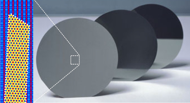
They have devised a method to grow graphene — the single-atom-thick carbon material — directly on top of silicon wafers. Graphene nanoribbons have a special advantage over the material when it’s in its more common form of a broad, flat sheet; namely, thin strips of graphene become excellent semiconductors, potentially outperforming silicon in transistor drive current and thermal conductivity.
“Compared to current technology, this could enable faster, lower power devices,” said Vivek Saraswat, a PhD student in materials science and engineering at UW-Madison.
The advance could enable graphene-based integrated circuits, with much improved performance over today’s silicon chips.
“The main advantage of graphene nanoribbons is that more electrons can travel through them, compared to silicon so you can make faster chips that use less energy,” said Mike Arnold, a professor of materials science and engineering at UW-Madison and a world expert in graphene growth.
Arnold is pioneer of a strategy to lay down long, thin strips of graphene — structures known as nanoribbons — on top a material called germanium.
While useful, germanium isn’t a widely used semiconductor, which means it can’t form the basis for computer chips.
Meanwhile, other researchers have not been able to overcome a major barrier in layering graphene nanoribbons onto silicon. Graphene reacts with silicon to form an inert and less useful compound called silicon carbide.
Arnold’s group has developed a method to avoid that obstacle. Instead of attempting to grow nanoribbons directly on silicon, they first grew a thin layer of germanium on top of silicon, followed by growth of nanoribbons. The thin germanium layers on silicon protected graphene from reacting with silicon yet didn’t interfere with the nanoribbons’ semiconducting capabilities.
It’s an important first step toward creating graphene-based integrated circuits. And because the base layer is composed of silicon, the graphene nanoribbon technology can be easily integrated into existing electronic/computing components.
“Our vision is to integrate graphene with existing semiconductor technology,” Arnold said.
One advantage of their synthesis approach is that it takes advantage of a scalable, industry-compatible chemical vapor deposition technique. Now, they’re working to improve the precision with which they lay down their nanoribbons so that they can achieve the complex patterns found in modern computer chips.
“We are using a few strategies to control the width and the orientation for the nanoribbons,” Arnold said. “We have a few really cool ideas.”
University of Wisconsin-Madison
www.uwm.edu
– Edited by Chris Vavra, production editor, Control Engineering, CFE Media, [email protected]. See more Control Engineering industrial PC stories.