This tutorial on closed-loop control for optical communications can be appropriate for other control applications. The amplifier used in fiber-optic communication behaves differently than an electronic amplifier; to maintain a constant gain requires using a type of closed-loop control – automatic gain control (AGC).
Automatic gain control insights
- Embedded in a fiber-optic communications signal integrity challenge is a solid opportunity to adapt feedback and feed-forward control.
- Fiber-optic communication amplifiers require using a type of closed-loop control, automatic gain control (AGC), to maintain a constant gain.
- Equations, examples and nine figures work resolve challenges, applicable to other control applications.
While the control process is an integral part of any industrial system, you might be surprised that the same applies to the optical (and other) communication systems as well. This article, while useful for the software engineers designing such communication systems, also helps engineers and designers working in different (industrial) fields, as many problems, challenges and solutions can be very similar.
Optical communications are part of everyday life along with wireless and satellite communications. Internet, television and telephone connections over long distances are unthinkable without optical fibers. Long-haul optical networks cross countries and oceans. While the advantages of such optical communications are well understood (no electrical interference, for example), its practical realization is as demanding as many other technically complex physical systems.
The optical (light) stream inside fiberoptic communication cables degrade with distance. Intensity decreases and overall quality deteriorates due to dispersion. Each optical stream combines more than one hundred separate, monochromatic (invisible) light streams of a slightly different wavelength, each binary (on/off) modulated with frequency equivalent to tens of GHz. This type of optical communication is known as the dense wavelength division multiplexing (DWDM) system. Using DWDM a tiny optical fiber can transmit data consisting of several Tbits/sec. (A stream of around 6.5 Tbits/sec can represent 100,000,000 simultaneous phone calls.)
After approximately 80 to 100 km, such a “degraded” optical signal must be fixed. There are optical ways to decrease degradation due to dispersion, and fortunately, the signal intensity can be amplified optically as well. Otherwise, the optical signal would have to be completely decoded (that is, converted to those multiple electrical signals) and consequently encoded back to the optical stream. Fortunately, that’s only required after the optical signal travels a thousand kilometers or so. Usually this is done in the hubs, where certain data channels are dropped and some others added.
Hardware at the core of this control equation
What kind of amplifier can be used to amplify such a complex optical signal? We will concentrate on one complex and useful type of optical amplifiers, among many. The erbium-doped fiber amplifier (EDFA) uses a short loop of a special, erbium-dopped optical fiber inserted between the incoming and outcoming signal fiber of the optical network. EDFA uses a special laser which adds energy to this erbium-doped fiber loop. This energy form is light with a slightly different wavelength than of those optical channels. This added energy exhibits a very interesting phenomenon. It excites the valence electrons in the erbium atoms which, when returning to their original orbits, release photons. And those photons can join and amplify the modulated light stream photons in the traveling signal.
The EDFA amplifier behaves differently than an electronic (operational) amplifier. While the electronic amplifier maintains constant gain (determined by the ratio of the input and feedback impedances) regardless of the amplitude of the input signal, the EDFA amplifier tends to keep rather a constant output power level, determined by the laser “pump” power. Maintaining a constant gain requires using a closed loop control – automatic gain control (AGC).
Brief analysis of EDFA amplifier
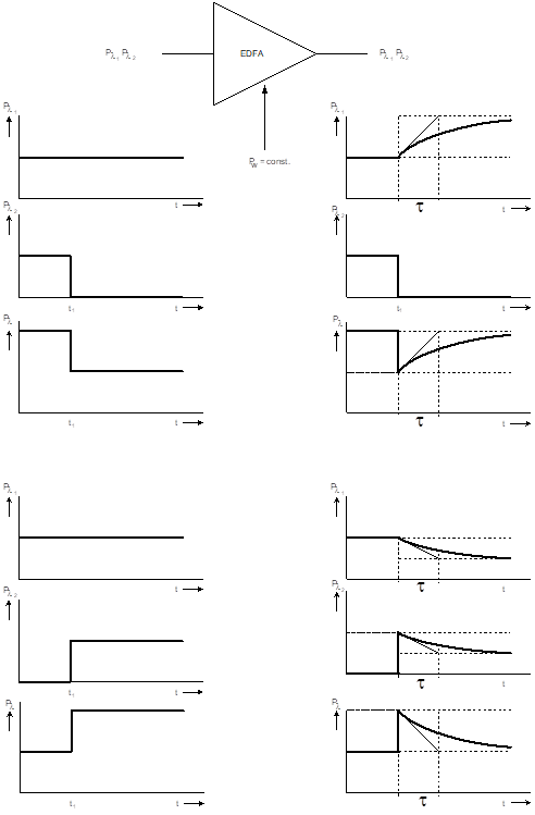
Figure 1 explains behavior of a non-regulated (one using constant laser pump power) EDFA amplifier. The picture shows how EDFA promptly reacts to any sudden changes of input power, however, in its steady state, it tends to maintain the same constant power, which depends only on the pump power. Just to clarify, a sudden change of input power occurs whenever some communication channels are added or dropped, which is a normal situation in such communication networks.
From this point of view, the EDFA amplifier behaves like a derivative member with the first-order lag, that is, a high-pass filter. It means that the high frequency input power changes pass through the amplifier almost untouched, but the constant or low frequency optical signals are filtered out, and the steady state power level depends only on the pump power. The time constant, T, with which the EDFA amplifier reacts to the step function of the input power, is not a constant value, but it depends on the current output power of the amplifier. At the higher output powers, this time constant is lower (the amplifier reacts faster). The variation of the time constant in a working output power range is rather high, from milliseconds to almost 10 microseconds.
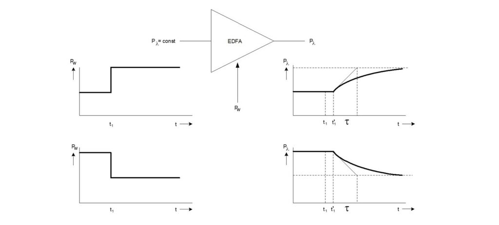
Figure 2 shows how the output power of the EDFA amplifier depends on the applied pump power. From this point of view the EDFA amplifier behaves like a first order, low-pass filter. Its time constant, T, is again variable and it depends on the current output power. Practically, T is the same time constant, which governs the output/input power transfer function.
As an integral part of the pump power-to-output power transfer function is the delay, t1-t1. This delay represents time, during which excited electrons stay in the high (excited) level before they move to the so called “meta-stable” level. This is a phenomenon typical for laser pumps of certain wavelengths. This time delay can be few microseconds. (More about the basic physical principles of laser-based optical communication is available in EDFA-specific literature.)
Synthesis of automated gain control system
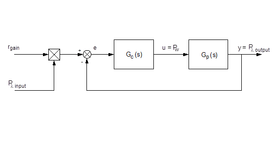
Figure 3 shows a basic block diagram of a closed-loop control system capable of maintaining the constant optical gain of the EDFA amplifier. The reference (target) gain value, rgain, at first multiplies the value of the input power, Plinput, to provide a required output power value. This value is then compared with the actual output power value, Ploutput, to provide the regulation error, e. The regulation error is processed by the controller with the transfer function, Gc(s). Output of the controller is an actuating variable, u, which is a desired pump power, Pw. The controller should be of the PI type, because a steady state error of zero is required. Adding the derivative member to the PI controller would speed up the response of the whole controlled system, however derivative members in a noisy environment can cause a lot of damage. However, we will not give up adding a derivative member completely. As you will find later, such a derivative member but with a first-order lag (real derivative or filtered derivative) will be added in the common, feed-forward plus feedback branch.
Digital PI controller has the transfer function, Gc(s)

The transfer function of the EDFA amplifier (output power versus pump power), Gp(s), can be approximated by a first order transfer function. Such approximation seems to be adequate for finding the appropriate control parameters. The time constant, T, is in the range from 10 microseconds to 10 milliseconds.
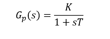
However, the t1-t1 delay shown in Figure 2 will be taken into consideration. The control parameters, a proportional constant, KP, and an integral constant, KI, will have to be set up such a way that the KP/KI ratio will equal to the time constant T thus cancelling it.
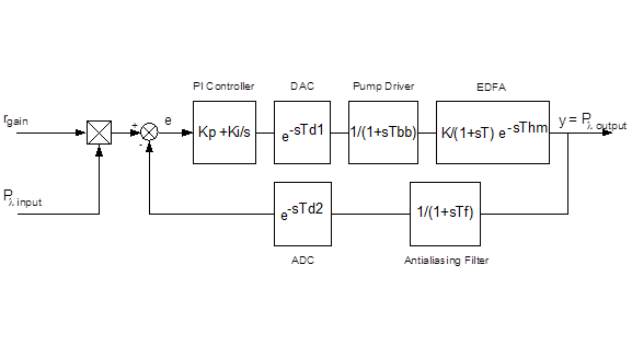
The accurate analysis of the controlled system should include the whole processing chain including antialiasing filters, A/D and D/A converters etc., as it is depicted in Figure 4. Why? Because if the feedback action runs so often (like every microsecond), any, even relatively small delay, must be taken into account as it may have negative impact on the overall system stability.
With the sampling/processing frequency around 1 MHz, the antialiasing filter (at least of a second order) should have the cut-off frequency, Tf, only marginally lower than the half of the sampling frequency, not to have any impact on the stability of the closed loop. The time delays of the D/A, Td1, and the A/D, Td2, converters are negligible, similarly like the time constants (better say “slew rates”), Tbb, Tf, of the op-amps used in the pump driver and anti-aliasing filter (not shown in Figure 4).
As we already know, the time constant of the controlled system (laser pump), T, is not a constant value through the whole working range of the output powers of the amplifier. In addition, it depends on wavelength of the amplified optical signal. And there might be another time (transportation) delay, Thm, (t1-t1 in Figure 2), which also must be accounted for.
The control parameters KP and KI should be set so that the time constant, T, of the plant transfer function, Gc(s), will be cancelled under any situation. This calls for an adaptive control, which would modify the control parameters according to the current value of the output power of the amplifier. To modify the control parameters, the current output power must be continuously monitored and used as the input either to a look-up table or to a polynomial and to get the desired KP/KI ratio.
If a look-up table is used, it makes sense to have an entry point for each digitized power value. In the case of a 12-bit A/D converter, 4096 entry points would be needed. Dependence of the time constant on the output power value very closely follows a hyperbolic function, so instead of the look-up table a direct calculation could be used. Though this calculation can be simplified to a single division, the look-up table can deliver results far faster than applying division.
How fast is fast enough in the feedback control loop?
As you can see, the above-described feedback-based AGC system is nothing special if it runs fast enough. The question is: How fast is fast enough? This depends on the time constant, T, of the amplifier. The worst case is when it is around 10 microseconds. It means that the feedback control loop should be running at least every 1 microsecond to be capable of a proper output power maintaining without any transient “glitches.”
If the classic feedback loop is combined with the feed-forward control, it does not need to run so often; 2 – 4 microsecond period is quite adequate. However, the feed-forward control should be very fast, running every few hundreds of a nanosecond. Such a control system can achieve much better transient performance than a control system based on feedback only.
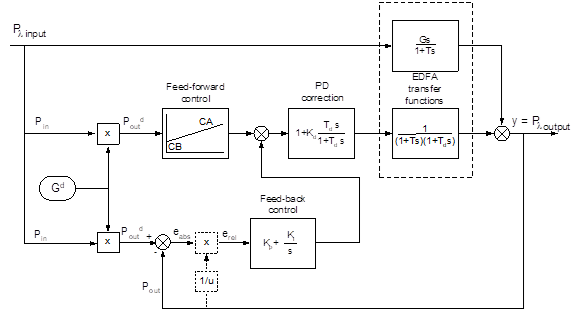
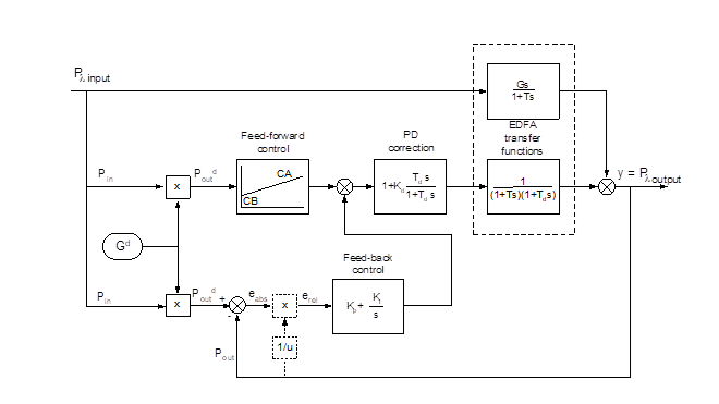
Figure 5 shows such a combined, feedback plus feed-forward AGC system. It is described in the “s” plane, as a time-continuous system, though its practical implementation can be any combination of the analog and digital technique. The feed-forward and the feedback branches are independent, and the only common information is the gain set point, Gd. Even the input power, Pin, measurement could be implemented independently in both subsystems with a more filtered signal/information used by the feedback controller. The feed-forward control can be implemented by:
- The same MCU (DSP) used for the feed-back loop implementation
- An analog circuitry
- A field programmable gate array (FPGA).
The first option is suitable, because today’s MCU/DSP can be very powerful. However, using the analog circuitry might be useful for feed-forward branch implementation as well. It does not require any A/D conversion of the input optical power, its “calculation” speed is extremely high (tens of nanoseconds), and it can be cheap. However, using an FPGA is the recommended approach, fast enough to make all calculations within hundreds of nanoseconds. The FPGA can be used for the optical powers measurement as well.
Classic feed-forward, feedback control
In Figure 5 is the feed-forward control branch depicted as a “transfer function” of the desired output power, Poutd, into a corresponding pump power, determined by the pump gain, CA, and the pump offset, CB. In practice, the following PD correction block is an integral part of the feed-forward branch as well.
Look more closely at the control system diagram in Figure 5. Basically it is another variant of a “classic” feed-forward plus feedback control system. Notice the top branch in the diagram. It doesn’t belong to the controller itself, it represents the input-to-output power transfer function of a typical EDFA as shown in Figure 1. The desired output variable, Pout d, is obtained as a product of the input power, Pin, value and a desired gain value, Gd. This is what defines the feed-forward branch. In the feedback control branch, at first the absolute regulation error, eabs, is being calculated. But what “feeds” the PI control block is a relative value of the regulation error, erel. Why? Because at the optimally tuned system the KP/KI ration should match the value of T. Since the dominant time constant of the EDFA transfer function, T, is inversely proportional to the output power, Pout, of the amplifier, the KP/KI ratio should also be a function of Pout-1. This can be achieved, if instead of processing an absolute regulation error
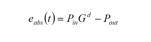
a relative regulation error can be calculated as follows.
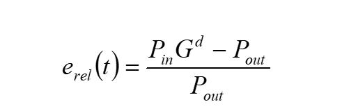
As mentioned, even though this is an elegant approach to take into account the variable time constant, T, value, in practice it is still preferable to use a “variable” Kp constant (or the KP/KI ratio) picked up from a look-up-table.
The contributions of FF and FB are then combined and could be applied to the pump driver. However, a real EDFA transfer function (output power versus pump power function) contains a transportation delay, Thm, as shown in Figure 4. In Figure 5 it is for simplicity replaced by an additional first order, low-pass filter with the time constant Td. Why? The effect caused by a transportation delay can’t be compensated by any means. System would have to be able to predict any input changes and to start to act before such change occurs, which obviously is not physically possible. But it is simple to compensate the effect of the first order low-pass filter – just use a derivative with the first-order lag (filtered derivate) block. And this is exactly what the PD correction block contains.
Optical power measurement
To control the EDFA amplifier, its input and output optical power must be continuously measured. For that purpose, a small but fixed amount of the light is “tapped” from the optical fiber cable, leading to and from the amplifier. Tapped optical powers are monitored by photodetectors. The most widely used photodetectors are avalanche photodiodes (APD) and positive-intrinsic-negative (PIN) photodiodes. The optical signal detected by a photodetector varies in a very wide range. Its dynamic range can easily reach 30 to 40 dB. It means that the output voltage provided by the photodetector can vary between, for example, 3000 mV (maximum output level) and 0.3 mV. It would not be possible to sample and digitally process such widely changing signal without additional analog processing.
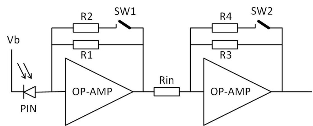
For PIN diodes two-stage electronic amplifiers are widely used. The first stage, called a transimpedance amplifier (TIA), is a current-to-voltage converter. The second stage, usually called post TIA (pTIA) is just an additional voltage amplifier. Together they can provide two (or more) different gain settings. For example, one such the TIA plus pTIA solution shown in Figure 6 provides 4 different gain settings.
The TIA + pTIA output voltage is usually unipolar, in the range between 0 and 3.0 V, for example. However, for correct power reading this range must be limited by around 5% on each side of the range. If the current voltage value is out of this range, the next higher or lower gain must be set. The minimum acceptable voltage, Vmin, then might be something like 150 mV and the maximum acceptable voltage, Vmax, might be 2850 mV. The output voltage of such TIA + pTIA circuitry is periodically sampled and digitized by a fast, 12-bit A/D converter. The Vmin and Vmax voltages are represented by the corresponding Nmin and Nmax 12-bit integer numbers. Those Nmin and Nmax values are used by the control algorithm to decide when to change the TIA + pTIA gain (increase or decrease).
Let’s look at a simple algorithm of TIA + pTIA gain control, which can be later on combined with the EDFA gain control. First, any A/D reading has to be calibrated. The sole purpose of the signal calibration is to eliminate effect of varying gain and offset of analogue circuitries of different op-amps and their resistors, and different sensitivity of the PIN diodes.
For the numerical reading, ADCsampleValue, the following formula holds:
ADCsampleValue = MeasuredPower * TotalGain + Offset
where
MeasuredPower is a real power tapped from the input/output of EDFA,
TotalGain is a numerical value, which includes the gains of TAP, PIN, TIA, pTIA and A/D converter,
Offset is a numerical value, which the DSP would see as ADCsampleValue if the current power value at the TAP was zero.
So the measured power will be calculated as:
MeasuredPower = (ADCsampleValue – Offset) / TotalGain
Each TIA + pTIA circuitry has four gain settings. Their entire gain range should cover the entire expected power range, 40 dB, for example. So, going from one gain switch setting to the next one should represent 10 dB of optical power increase/decrease.
Practically it means there will be four offset and four gain values, one set for each combination of the switches SW1 and SW2.
| SW1 | SW2 | TotalGain | Offset |
| ON | ON | G0 | O0 |
| ON | OFF | G1 | O1 |
| OFF | ON | G2 | O2 |
| OFF | OFF | G3 | O3 |
These values will have to be downloaded to the controller after power up and when any of these values has changed.
The switching values Nmin and Nmax corresponding to the minimum and maximum working voltages at the output of TIA + pTIA might be defined as (software) constants.
EDFA control algorithm
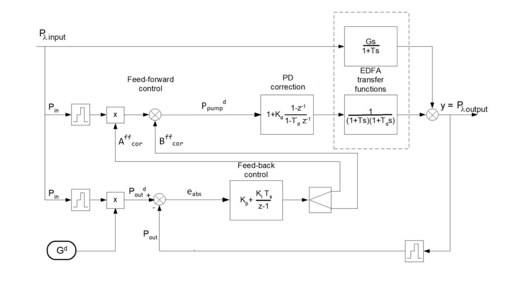
As we were already discussing possible EDFA control implementations, let’s concentrate on one, the simplest implementation. In this case, the feedback and feed-forward branches are implemented digitally. This implementation is shown in Figure 7.
A first change from Figure 5 are additional “sample-and-hold” blocks, which are fast A/D converters following the TIA + pTIA circuitries. These additions are necessary, as the block diagram in Figure 7 represents a digital/discrete control block diagram, not a continuous one shown in Figure 5.
The PI control block in the feed-back branch and the PD correction block in the feed-forward branch are shown in their discrete forms. Ts in the PI control block represents the sampling period, though it is not used in the calculations, it’s considered to be a value of 1. However, the Kiparameter must be modified to consider this sampling-period value. For simplicity, the sampled input power can be shared between the FB and FF branch, though it is desirable for the feed-forward branch to run more often (like 4-times) than the feedback correction. Still both branches could use the same input power sampling and reading, just for the feedback correction that power reading could go through a better filter.

The actual control algorithm implementation is derived from the second-order biquad infinite impulse response (IIR) filter, as shown in Figure 8. This is the shortest/fastest implementation of the proportional-integral-derivative (PID) compensation. The canonical IIR filter section is best described by the following two difference equations.
d(n)=x(n)+A1 d(n-1)+A2 d(n-2)
y(n)=B0 d(n)+B1 d(n-1)+B2 d(n-2)
Such implementation requires less memory space – instead of usual four state variables (two previous error and output values), they must remember only two state variables, d(n-1) and d(n-2). For more information look at the Control Engineering article on PID correction-based control system implementation.
However, as we use a simpler PI controller, the second delayed state variable, d(n-2), with the coefficients A2 and B2 will disappear from the calculations, and the equations will be simplified:
d(n)=e(n)+A1 d(n-1) (E1)
u(n)=B0 d(n)+B1 d(n-1) (E2)
where A1 equals 1, B0 equals T/2.KI + KP and B1 equals T/2.KI – KP, where T is a sampling period.
The algorithm implementation needs 2 additions and 2 multiplications, and it needs only one internal state, d(n-1) to remember. This is the minimum possible calculations required for such a PI control algorithm implementation. And this is extremely important for AGC applications such as the EDFA control, because this control loop should run optimally once every microsecond.
In the implementation of this algorithm, instead of clamping the actuating value, u(n), a value of d(n) must be clamped before it is used in the second equation (E2). Find more about why clamping is important in the Control Engineering article: From simulation to computer-aided design of control systems. Clamping of the d(n) value is identical with clamping of the contribution of integral member output, because d(n) represents accumulation of the regulation error, e, as you can see from E3:

Substituting (E3) in (E2) will give

After simplification we get

Equation E4 evidently describes a PI controller with a trapezoidal integration.
Using Equations E1 and E2, the PI Control algorithm (in a C-like pseudo code) can look as follows:
/* Calculate calibrated Input and Output Powers from input/output ADCreading values;
Required Output Power = Target Gain * Input Power;
RegError = Required Output Power – Output Power; */
// Feed-back branch
Kp = *LUTptr[OutPower]; // Kp retrieved from LUT *
dn = RegError + dnPrev;
if (dn > DNMAX)
dn = DNMAX;
if (dn < -DNMAX)
dn = -DNMAX;
un =( T/2*Ki+ Kp) * dn + ( T/2*Ki – Kp) * dnPrev;
Affcor = fng(un); // split un into (corrected) Aff and Bff
Bffcor = fno(un); // for splitting use fng() and fno() functions **
dnPrev = dn;
// Feed-forward branch, corrected CA and CB parameters
pumpPwr = inpPwr * Affcor + Bffcor;
// Common branch is a proportional-derivative block
u = x + a0*x + a1*xPrev + b1*uPrev; // x = pumpPwr, a0, a1, b1 ***
xPrev = x;
uPrev = u;
// And finally:
Apply calculated u value via DAC as a pump power correction; ****
*) Please notice that we use an absolute value of the regulation error, not the relative one. This is because we made the Kp parameter dependent on the current value of the output power. Using a look-up-table even with 4096 entries is still preferable solution than one floating point division.
**) Output of the PI control block can be added as a simple correction (offset value) of the feed-forward branch contribution, which itself represents a desired pump power, Ppumpd, value. However, in such very fast AGC systems it is better to split the feed-back correction into two parts, one correcting the gain parameter in the feed-forward branch, and the other part correcting the offset. What are those gain and offset parameters? The gain definitely involves a desired EDFA gain value Gd. But this is not all. The desired output power, Poutd, which is a product of the actual input power value, Pin, and a desired gain, Gd, must be transformed to a desired pump power value. This transformation is a simple linear function consisting of a certain pump “gain” value and a pump “offset” value. In Figure 5 those are the CA and CB parameters of the feed-forward branch. Those two parameters are specific to the laser device and usually have to be found experimentally. In Figure 7 the Affcor and Bffcor parameters represent a corrected feed-forward gain value and the corrected feed-forward offset.
Regarding a possible splitting (distribution) function of the feed-back correction, just keep the principle, the lower input power the higher portion of the correction goes towards the offset modification, and the higher input power the higher portion of correction goes towards the gain modification. Doing so we tune the laser pump gain and offset values “on the run,” as their initial estimation might not be best. Why it is so important to know the best possible laser pump gain and offset values? The closer those values are to the actual laser pump parameters, the more precisely will be feed-forward branch able to cope with any sudden input power change, thus leaving for a (slower) feed-back branch only minor corrections.
***) The coefficients a0, a1, b1 calculation is explained at https://www.controleng.com/from-simulation-to-computer-aided-design-of-control-systems.
****) There is no way to use any other type of digital-to-analog conversion than using a linear D/A converter. Its efficiency is poor but fortunately we are talking about watts of power, not kW. The PWM driving method would require an extremely high modulation frequency, causing significant noise generation/disturbance.
TIA control algorithm
What we haven’t covered in the previous chapter is the TIA control. And it must be included in the EDFA control process. Having valid input/output power values is essential.
TIA control can be implemented as one software module with the data calibration. After power-up the TIA control switches SW1 and SW2 will be set to provide the minimum gain. Since then, after each measurement the measured value is compared with the low and high switching value, and the gain is adjusted accordingly:
Raw 12-bit ADC reading (minus the offset value) compare with the Nmin and Nmax values. Nmin can is a value equivalent to 5% of 4096, while Nmax can be a value equivalent to 95% of 4096, for example.
In the next program fragment such a simple TIA gain control algorithm is implemented. The initial switch combination, sw, is SWmin, which corresponds to the minimum gain setting, 0x00. SWmax corresponds to the maximum gain setting, 0x03. The initial switching value is calculated as:
SwitchingValue = (ADCsampleValue – offset[SWmin]);
In the fastest (i.e. most frequent) ~ feed-forward control loop run the following code:
if(SwitchingValue < Nmin) {
sw++; // increase gain switch setting
if(sw > SWmax)
sw = SWmax; // maximum gain switch (0x03) setting
}
else if(SwitchingValue > Nmax) {
sw–; // decrease gain switch setting
if(sw < SWmin)
sw = SWmin; // minimum gain switch (0x00) setting
}
SwitchingValue = (ADCsampleValue – offset[sw]);
MeasuredPower = SwitchingValue / TotalGain[sw];
Of course the switches used must be of the fast, silicon/semiconductor type with a fast settling time (~ 10 nsec). The same procedure as shown here can be used for each input and output optical power measurement point.
Finalizing control firmware implementation
It is obvious that both AGC (namely its feed-forward branch) and TIA control algorithms are suitable to combine into one software implementation. As a processing unit any (even fixed point) digital signal processor (DSP) works best. Very often EDFA amplifiers are built as dual-stage amplifiers. A DSP whose core can run in the simple instruction multiple data (SIMD) mode is the most suitable. In such a processor the same processing runs in parallel for two separate sets of data. One set of data belongs to the first stage, and the second one belongs to the second stage of a dual-stage EDFA amplifier. This of course can’t be applied to the TIA control algorithm, as both stages work with different optical power values, which may require different TIA switches.
The DSP-based digital controller, though it can work autonomously, is usually integrated into a more complex system, a circuit pack. Circuit pack is usually controlled by another central processing unit (CPU) or main processing unit (MCU). From the point of view of DSP this CPU acts usually as a host processor. The host is responsible for loading the firmware into DSP after power-up, providing initial parameters (for example PI constants) and periodically providing various operating parameters like the target gains. DSP usually communicates with the host via a suitable serial port, for example serial peripheral interface (SPI) or a parallel host direct memory access (DMA) channel. All these communication procedures can run as the background process. If the data exchange with the host is relatively rare, for example once per few milliseconds, the SPI (or other communication) controller will generate an interrupt whenever its receive buffer has obtained new data from the host. Those interrupts will not interfere with 1 microsecond interrupts generated by the internal timer for the main control loop.

Figure 9 shows such a dual-stage optical amplifier, which is a part of a circuit pack.
The circuit pack, in addition to the optical amplifier contains as a minimum the host part, which provides connection with a user. But there might be additional optical devices built in (Figure 9 shows a dispersion compensation module (DCM). This optical device is an independent unit from EDFA, just belonging to the same circuit pack. It is usually placed between two stages of the optical amplifier.
Another optical device shown in Figure 9 is a variable optical attenuator (VOA). This one is an integral part of EDFA, so it must be controlled with the amplifier stages. Its purpose is to maintain (together with the gain flattening filter (GFF)) a desired profile (tilt) of the individual amplified optical channels ~ light streams with a different wavelength.
There are other devices, like thermoelectric cooler (TEC), which is an integral part of the EDFA as well, and its firmware and a small heater, maintain constant temperature of the enclosure where the erbium-dopped fiber loop resides. All those devices are “slow,” thus the EDFA processor can devote 90% of its power to the fast, laser pump control process.
The EDFA shown in Figure 9 is complex. Notice the second stage (B), it itself represents a dual-stage amplifier though controlled as a single stage. There could be similar architectures with more powerful amplifiers having even several laser pumps running in parallel in the final stage. Another important fact might be using assembly language for the writing the most time critical procedures. Such an approach requires far more attention throughout the entire firmware design and implementation phase.
Compared to simple C programming, the mixture of C programming and in-assembly written routines along with their mutual interactions are a much more demanding software engineering job. It requires full knowledge of all hardware and programming resources of the MCU/DSP used. Maintenance (further modifications) of such a mixed load is very difficult. My advice would be to avoid assembly programming if possible. Select the most powerful MCU/DSP unit, so it wouldn’t have a problem running the longer load created by the C compiler quickly enough for the application.
More advice, applicability for other control applications
Other control system applications may benefit from the optical communications control challenges and solutions discussed here. After more than 25 years designing industrial control systems, I joined Nortel, a major optical communication company at that time. The parallels for industrial control system designers are many.
First, the physical principles of the project must be understood. This is the first and inevitable step in any engineering project. Fortunately, scientists and other specialists have already studied and discovered all important phenomena and features of most design engineer project challenges. Find and study suitable literature. Once you understand the subject of your design activities, continue with system analysis followed by the synthesis and implementation. Find more help for control software engineering processes in the articles cited.
Peter Galan is a retired control software engineer. Edited by Mark T. Hoske, editor-in-chief, Control Engineering, WTWH Media, [email protected].
Keywords
Optical amplifier control case study, feedback and feed-forward control
Consider this
What in this feedback and feed-forward control project help your next control system implementation?
You also might like
https://www.controleng.com/from-simulation-to-computer-aided-design-of-control-systems/
https://www.controleng.com/introduction-to-control-software-engineering-better-automation-designs/